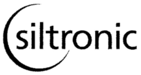
siltronic Logo (WIPO, 07/08/2004)
Protect this trademark from copycats!
With our trademark monitoring alerts, you are automatically notified by email about copycats and free riders.
The International trademark siltronic was filed as Figurative mark on 07/08/2004 at the World Intellectual Property Organization.
Logodesign (Wiener Klassifikation)
#Lines, bands #Letters presenting a special form of writing #Curved lines or bands (except A 26.11.13)
| Trademark form | Figurative mark |
| File reference | 849069 |
| Register number | 30405445.3/01 |
| Countries | 


|
| Base trademark |
 No. 304 05 445.3/01,
March 4, 2004
|
| Application date | July 8, 2004 |
| Expiration date | July 8, 2024 |
Trademark owner
Einsteinstraße 172
81677 München
DE
81677 München
DE
Trademark representatives
Johannes-Hess-Straße 24
84489 Burghausen
DE
goods and services
01
Chemical products used in industry, science, photography,
agriculture, horticulture and forestry; silanes;
hydrochloric acid; conductive and semiconductive, doped and
undoped organic polymers; inorganic elements and compounds
in form of hyperpure crystals; gallium-gadolinium garnet;
doped and undoped, polycrystalline and monocrystalline
inorganic semiconductor material, particularly in the form
of crystals, granules and powders, in sawed, lapped,
polished, etched and coated form; doped and undoped,
polycrystalline and monocrystalline inorganic semiconductor
material, particularly in the form of rods, tubes, sheets
(wafers) and moulded bodies, in sawed, lapped, polished,
etched and coated form included in this class; substrates
coated with semiconductor material in the form of sheets
(wafers), rods, tubes, granules and powders; substrates
coated with semiconductor material in the form of moulded
bodies included in this class; hyperpure silicon for the
electrical and electronic industries; monocrystalline
silicon in the form of rods, blocks, sheets (wafers), and
powders; polycrystalline silicon in the form of powders and
granules; polycrystalline silicon in the form of blocks,
sheets and moulded bodies included in this class
09
Organic semiconductors; doped and undoped, polycrystalline
and monocrystalline inorganic semiconductors, particularly
in the form of rods, tubes, sheets (wafers) and moulded
bodies, in sawed, lapped, polished, etched and coated form
included in this class; substrates coated with
semiconductors in the form of moulded bodies included in
this class
Trademark history
| Date | Document number | Area | Entry |
|---|---|---|---|
| December 2, 2016 | 2017/20 Gaz | US | RAW: Partial Invalidation |
| July 8, 2014 | 2014/28 Gaz | Extension | |
| December 5, 2006 | 2007/46 Gaz | US | Decision on opposition |
| September 11, 2006 | 2007/48 Gaz | KR | Decision on opposition |
| June 7, 2006 | 2006/28 Gaz | NO | RAW: Protection Granted |
| April 27, 2006 | 2007/34 Gaz | JP | Decision on opposition |
| March 7, 2006 | 2006/12 Gaz | KR | Rejection |
| February 27, 2006 | 2006/12 Gaz | SG | RAW: Protection Granted |
| December 19, 2005 | 2006/3 Gaz | GB | RAW: Protection Granted |
| December 1, 2005 | 2005/48 Gaz | JP | Rejection |
| November 15, 2005 | 2005/47 Gaz | IE | RAW: Protection Granted |
| October 31, 2005 | 2005/45 Gaz | AU | RAW: Protection Granted |
| June 30, 2005 | 2005/27 Gaz | US | Rejection |
| July 8, 2004 | 2005/21 Gaz | DE | Registration |
ID: 14849069
 WIPO
WIPO